In modern manufacturing, many product failures cannot be identified by normal visual inspection. A component may look acceptable from the outside but still contain microcracks, contamination, poor filler dispersion, surface defects, coating failure or structural weakness. This is where SEM microscope analysis lab services in Chennai – Kiyo R&D Lab become valuable for industries that need accurate material investigation and failure analysis.
Scanning Electron Microscopy, commonly known as SEM, is used to study surface morphology, fracture behaviour, particle structure, micro defects and material characteristics at high magnification. Compared with a normal optical microscope, SEM gives better depth, clarity and surface detail, helping manufacturers understand the actual reason behind product performance issues.
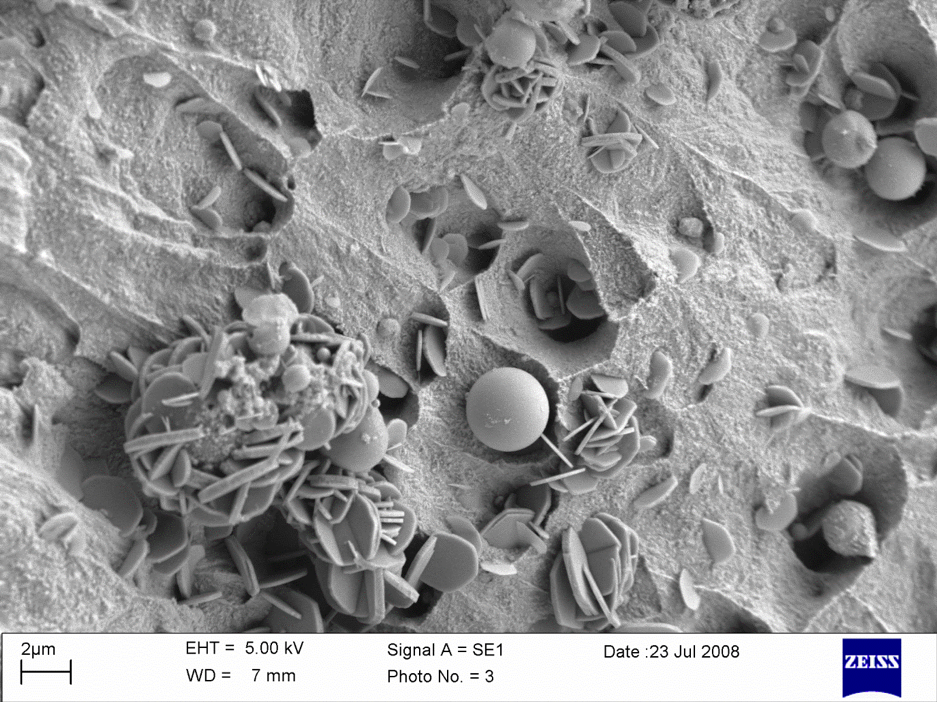
Kiyo R&D Lab provides SEM microscope analysis lab services in Chennai for plastics, rubber, composites, metals, coatings, powders, electronic parts and medical device components. The testing helps industries evaluate material quality, identify defects and support product development, quality control and customer complaint investigation.
SEM testing is commonly used for polymer crack analysis, rubber surface failure investigation, composite fiber evaluation, coating defect analysis, corrosion studies, contamination identification and microstructure examination. For manufacturers, this type of analysis gives clear technical evidence instead of assumptions.
Failure analysis is one of the most important applications of SEM testing. When a product fails during use, the reason may be linked to processing defects, material weakness, environmental exposure, poor adhesion, fatigue, brittle fracture or contamination. SEM microscope analysis helps identify these issues by showing the failure surface in high detail.
Through SEM analysis, industries can observe surface deformation, voids, porosity, microcracks, delamination, fiber pull-out, coating peeling, corrosion products and fracture patterns. This makes SEM microscope analysis lab services in Chennai – Kiyo R&D Lab useful for manufacturers who want to reduce repeated failures and improve product reliability.
Small microscopic defects can lead to major performance problems. SEM testing helps detect hidden defects that are not visible during routine inspection. These defects may occur due to raw material variation, improper processing, poor mixing, contamination, thermal damage, chemical exposure or mechanical stress.
At Kiyo R&D Lab, SEM analysis can support the evaluation of filler agglomeration, improper bonding, surface contamination, heat damage, interface failure, environmental degradation and poor dispersion of additives. This information is highly useful for R&D teams, quality departments and production teams.
Automotive, electrical, electronics and medical industries require reliable testing because even minor material defects can affect safety, durability and product performance. SEM microscope analysis lab services in Chennai help these industries investigate components at microscopic level.
In the automotive sector, SEM testing is useful for plastic interior parts, rubber seals, molded components, coating failures, corrosion studies and fractured components. In electrical and electronics industries, SEM analysis helps with PCB surface evaluation, connector failure analysis, solder joint examination, conductive coating analysis and contamination studies.
For medical device components, SEM testing can support surface cleanliness verification, polymer tubing analysis, catheter surface examination, particle analysis and material defect investigation. This makes SEM analysis a strong tool for industries where quality and consistency are critical.
Particle shape, size and surface texture can directly affect product performance. Powders, fillers, pigments, additives and coating materials often require SEM analysis to understand particle morphology and distribution.
SEM microscope testing can help observe particle size, shape, agglomeration, surface texture, contamination and distribution consistency. For industries working with polymers, coatings, composites and powders, this information helps improve formulation, processing and final product quality.
SEM is highly effective for fracture analysis because it helps identify whether a component failed due to brittle fracture, ductile fracture, fatigue, stress cracking, environmental stress cracking or thermal degradation. Understanding the fracture mechanism helps industries take corrective action in material selection, design or processing.
SEM analysis is also useful for corrosion studies. It helps observe oxidation layers, corrosion products, pitting, coating breakdown and surface degradation. For manufacturers handling metals, coatings and critical components, this level of investigation can prevent repeated product failures.
SEM combined with EDX analysis provides both high-resolution imaging and elemental composition details. SEM-EDX analysis is useful for identifying unknown particles, contamination sources, filler materials, corrosion residues and coating composition.
At Kiyo R&D Lab, SEM with EDX support helps industries perform foreign particle identification, elemental mapping, material comparison, coating analysis, heavy element detection and filler confirmation in polymer materials. This makes SEM microscope analysis lab services in Chennai – Kiyo R&D Lab more valuable for detailed industrial investigations.
Choosing the right laboratory is important because SEM analysis should not stop with images alone. Industries need technical interpretation, proper sample handling and meaningful reporting. Kiyo R&D Lab supports manufacturers with advanced material testing services, practical failure investigation and industry-focused reporting.
Kiyo R&D Lab supports plastics, rubber, composites, metals, coatings, electrical components, medical device parts and industrial samples. The lab is suitable for R&D validation, quality control, product failure investigation, supplier material verification and customer complaint analysis.
For companies looking for dependable SEM microscope analysis lab services in Chennai, Kiyo R&D Lab provides technical support with a focus on accuracy, clarity and industrial application.
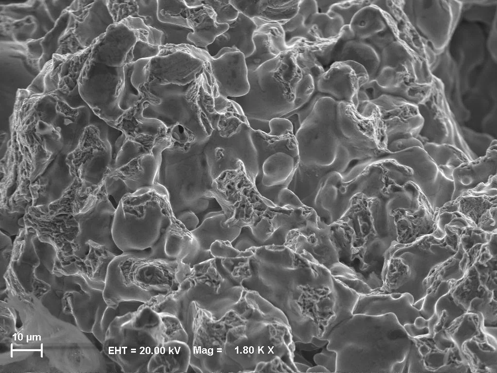
Sample requirements may vary depending on the material and purpose of analysis. Failed components, powder samples, polymer specimens, fractured parts, coated surfaces, metal sections, electronic components and thin film materials can be submitted for SEM analysis. The technical team will review the sample condition and suggest suitable preparation before testing.
Industries use SEM microscope analysis lab services in Chennai to identify microscopic defects that cannot be seen through normal visual inspection. SEM testing helps manufacturers understand the actual reason for product failure, surface damage, poor bonding, contamination or material inconsistency.
SEM analysis can be used for plastics, rubber, metals, composites, coatings, powders, fillers, pigments, electronic components, medical device parts and fractured industrial components. The suitability depends on sample condition and testing requirement.
Yes. SEM analysis is one of the most useful techniques for product failure investigation. It helps identify whether the failure is due to brittle fracture, ductile fracture, fatigue, stress cracking, corrosion, thermal damage, contamination or processing defects.
Yes. Kiyo R&D Lab provides SEM microscope analysis lab services in Chennai for industrial material testing, failure analysis, surface morphology evaluation, SEM-EDX elemental analysis and microstructure examination.
SEM analysis helps industries identify the exact defect or failure mechanism at microscopic level. This allows manufacturers to improve raw material selection, processing conditions, design quality, coating performance, supplier control and final product reliability.