Looking for a reliable SEM EDX analysis lab in Chennai? Kiyo R&D Lab offers precision SEM EDAX testing services for metals, polymers, coatings, and composites — covering surface morphology imaging, elemental composition mapping, and fracture analysis, tested to ASTM and ISO standards.
Scanning Electron Microscopy (SEM) produces high-magnification images of a material’s surface topology, while Energy Dispersive X-ray analysis (EDX, also called EDAX or EDS) identifies the elemental composition at any point on that surface — together giving a complete picture of what a material looks like and what it’s made of. Searching for a SEM EDX analysis lab in Chennai you can trust? As an ASTM/ISO-compliant SEM EDAX testing lab in Chennai, Kiyo R&D Lab helps automotive, electronics, plastics, and metal manufacturers investigate failures, verify coatings, and identify unknown particles or contamination. Our SEM EDX analysis Chennai clients rely on calibrated instrumentation for consistent, high-resolution imaging and elemental data.
High-magnification surface morphology testing reveals topology, texture, and micro-defects invisible to the naked eye.
Our elemental composition analysis Chennai manufacturers depend on identifies elements from boron through uranium at any imaged point.
Fracture analysis SEM Chennai engineers turn to when a component fails and the root cause needs microscopic evidence.
Our particle characterization testing sizes and identifies particles, fibers, and inclusions within a sample.
Foreign material identification SEM pinpoints contamination sources in raw materials and finished parts.
Our coating cross-section analysis measures layer thickness and verifies coating uniformity and adhesion.

SEM fitted with an integrated EDX detector — calibrated to ASTM/ISO reference standards before every scan.
Every SEM EDX testing service at our Chennai laboratory — from ASTM E986 testing to ASTM E1508 testing — is performed against internationally recognized standards, ensuring your reports are accepted by OEMs, auditors, and regulatory bodies. As an ISO 22309 testing lab, we cover both imaging and quantitative elemental analysis end to end.
| Standard | What It Covers | Typical Use |
|---|---|---|
| 1ASTM E986 | General practice for SEM beam characterization | Surface morphology imaging |
| 2ASTM E1508 | Quantitative analysis by EDS | Elemental composition |
| 3ISO 22309 | Quantitative & qualitative EDS point analysis | Elemental identification |
| 4ISO 16700 | SEM magnification calibration | Instrument calibration |
| 5ASTM E2809 | Particle characterization by SEM | Particle & fiber sizing |
| 6ASTM E1442 | Electron probe microanalysis practice | Composition mapping |
| 7IS 13360 (Part 7) | Indian standard for material analysis | Domestic OEM compliance |
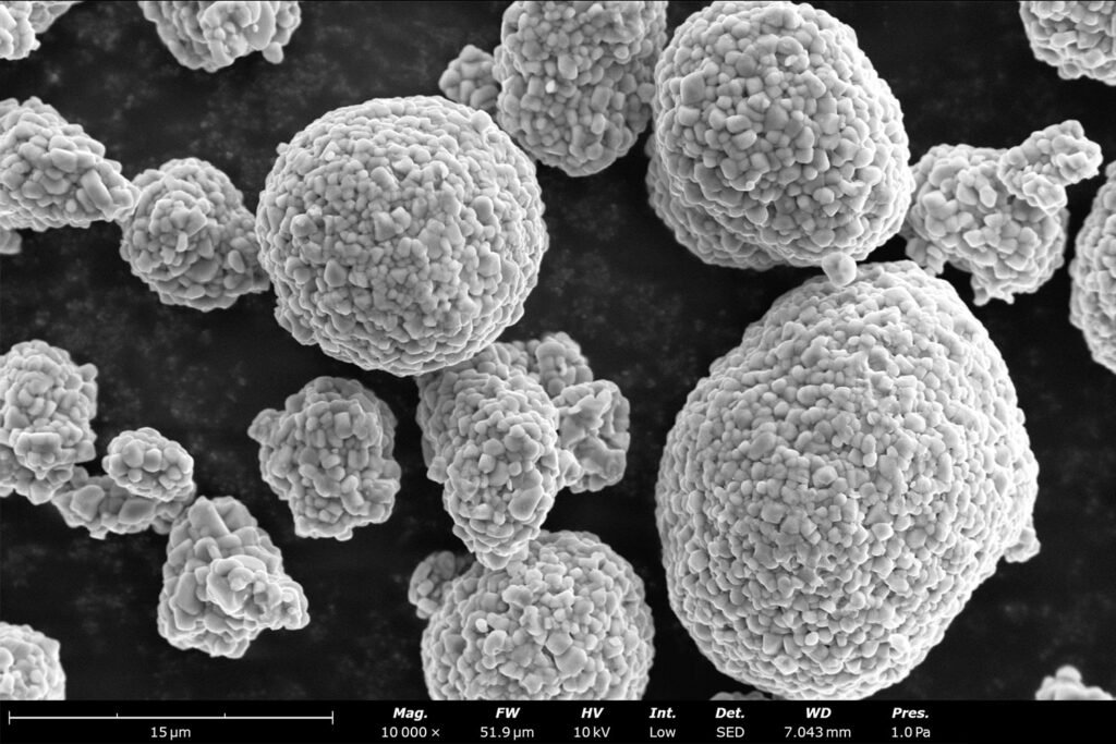
Our SEM EDX analysis lab in Chennai runs samples on a SEM fitted with an integrated EDX detector, giving high-resolution surface imaging and simultaneous elemental mapping for every test we deliver.
Share your material and applicable standard via call, WhatsApp, or email.
Get an itemised quote for your SEM EDX testing requirement within hours.
Calibrated SEM EDX instrumentation scans your sample per the chosen ASTM/ISO standard.
Receive a detailed report with SEM images and EDX elemental data, referenced to the exact ASTM/ISO standard requested.
Kiyo R&D Lab is a materials testing laboratory based in Chennai, with branches in Chrompet and Oragadam, serving automotive OEMs and Tier-1/2 suppliers, electronics manufacturers, and industrial manufacturers across the Tamil Nadu–Karnataka industrial corridor. Our SEM EDX analysis lab in Chennai is part of a broader testing capability spanning thermal analysis (DSC, TGA), spectroscopy (FTIR), mechanical, and electrical properties testing — giving manufacturers a single trusted partner for materials characterization end to end.
We work directly with engineering and quality teams to turn ambiguous “why did this fail” or “what is this material” questions into clear, standards-referenced answers — backed by calibrated instrumentation and analysts experienced in interpreting SEM images and EDX spectra for real production decisions.
ASTM/ISO-traceable calibration for every scan — accurate imaging and elemental data you can rely on.
Quick scheduling for urgent SEM EDX testing requirements in Chennai.
Skilled materials engineers interpreting every SEM image and EDX spectrum.
SEM EDX testing Chitlapakkam headquarters, plus Chrompet & Oragadam locations across Chennai.
Upfront, itemised quotations — no hidden costs.
ASTM, ISO, IS & OEM-specific SEM EDX test methods supported.
Our SEM EDX analysis lab in Chennai serves automotive, electronics, and manufacturing units across the city’s major industrial clusters — with easy sample pickup and drop-off from these areas.
Convenient sample drop-off for Chrompet-based electronics and plastics manufacturers.
Serving Oragadam’s automotive OEM and Tier-1/2 supplier cluster with fast turnaround.
SEM EDX analysis is one part of our full materials testing capability in Chennai. Explore related services below.
Fill the enquiry form below or call us directly — our team responds to every SEM EDX analysis lab in Chennai enquiry within one business day.
Fills your request and emails it straight to kiyo@kiyorndlab.com
We test metals, polymers, plastics, coatings, composites, and unknown foreign materials using SEM imaging and EDX elemental analysis.
Standard turnaround for SEM EDX analysis at our Chennai lab is 2–4 working days, with expedited options available on request.
EDX, EDS, and EDAX all refer to the same energy-dispersive X-ray analysis technique — the terms are used interchangeably across the industry and instrument manufacturers.
We test to ASTM E986, ASTM E1508, ISO 22309, ISO 16700, ASTM E2809, ASTM E1442, and IS 13360, along with OEM-specific methods.
Yes, our SEM EDX analysis lab in Chennai issues detailed reports with SEM images and EDX elemental spectra, referenced to the exact ASTM/ISO standard tested.
Call 90420 86986, message us on WhatsApp, or email kiyo@kiyorndlab.com with your material and standard requirement.
Yes — if you’re searching SEM testing near me, our Chitlapakkam HQ plus Chrompet and Oragadam branches put a SEM EDX analysis lab within reach across Chennai’s industrial corridor.