Need to see the surface of a material at microscopic scale, and know exactly which elements it contains? Scanning electron microscopy with EDS does both — high-magnification imaging plus elemental analysis from the same spot. A capable sem analysis lab in chennai turns that into clear answers about morphology, defects, coatings, and contamination. Kiyo R&D Lab helps you examine and identify your material with confidence.
From metals and coatings to plastics, powders, and unknown particles, our expert team delivers accurate imaging and elemental data, supporting interpretation, and clear, audit-ready reports you can rely on.
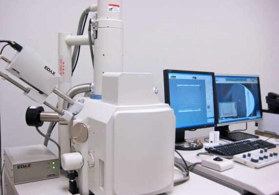
Your complete guide to SEM-EDS analysis at Kiyo R&D Lab
SEM stands for scanning electron microscopy — it scans a focused electron beam across a sample to produce high-magnification images that reveal surface texture, structure, and defects far beyond what a light microscope can show. EDS (energy-dispersive X-ray spectroscopy, also called EDX) is paired with it to identify which chemical elements are present at any point in the image. Together, a sem analysis lab in chennai gives you both a picture and a composition from the same spot.
That combination is powerful: you can see a defect, a particle, or a coating layer, then immediately find out what it is made of. It is one of the most versatile tools in materials analysis and failure investigation.
Our sem analysis lab in chennai covers the full range of routine SEM and EDS work across materials.
Morphology & texture.
EDS composition.
Failure investigation.
Particles & residues.
Thickness & make-up.
Where elements sit.
| Technique | What It Shows | Answers |
|---|---|---|
| SEM (imaging) | High-magnification image | What does it look like? |
| EDS (elemental) | X-ray spectrum | What is it made of? |
| EDS mapping | Element distribution image | Where are the elements? |
| Combined | Image + composition | Full surface picture |
Our sem analysis lab in chennai works best alongside complementary analysis methods, so you get structure, chemistry, and composition together.
| Technique | Adds |
|---|---|
| SEM-EDS | Imaging + elemental composition |
| FTIR | Polymer & organic identification |
| XRD | Crystalline phase & structure |
| TGA | Filler & composition by weight |
Combining SEM-EDS with FTIR or XRD gives a complete picture — ask us for a multi-technique material analysis package.
Based in Chennai with branches in Chrompet and Oragadam, Kiyo R&D Lab makes electron microscopy easy to access for the Chennai–Oragadam industrial corridor, with convenient drop-off and courier-friendly collection.
Looking for a sem analysis lab in chennai? Send us your sample and what you need to see or identify, and we’ll image, analyse, and report clearly.
Call 90420 86986 Request a QuoteExplore all our capabilities at www.kiyorndlab.com.
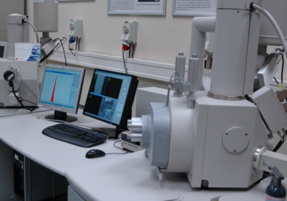
When you need to both see a surface and know what it is made of, SEM-EDS delivers both from one analysis. As a trusted sem analysis lab in chennai, we combine high-resolution imaging, elemental analysis, and expert interpretation to give you answers you can act on.
From a single particle to a full failure investigation, the team at Kiyo R&D Lab is ready to help. Reach out today and turn your sample into a reliable, audit-ready report.