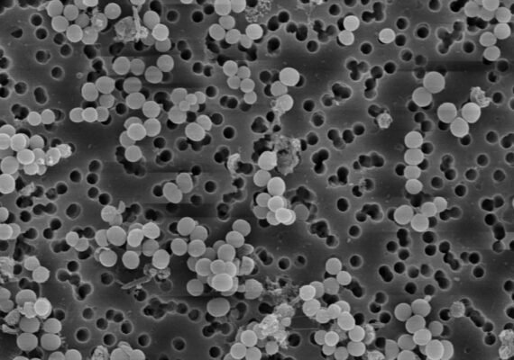
When you need to see a surface at high magnification and know exactly which elements are present, SEM-EDX is the technique that does both. It pairs scanning electron microscope imaging with EDS/EDX elemental analysis to reveal microstructure, composition, coatings, and contamination. Searching for a dependable sem-edx testing lab in chennai? Kiyo R&D Lab delivers clear images and confident elemental data for metals, plastics, electronics, and unknown particles.
From composition checks and coating analysis to defect and failure investigations, our expert team delivers sharp imaging, reliable EDS composition results, and audit-ready reports you can rely on.
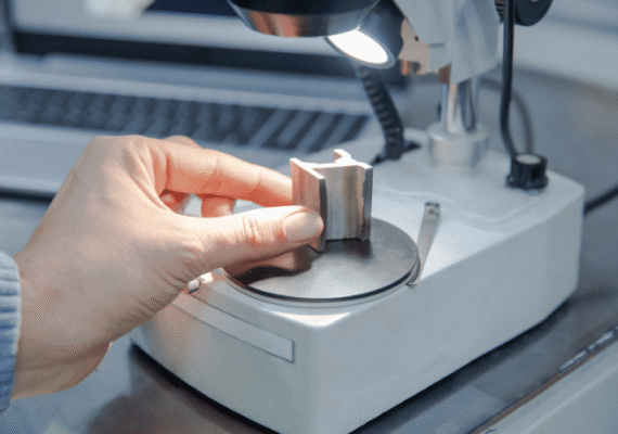
Your complete guide to SEM-EDX testing at Kiyo R&D Lab
SEM-EDX combines two techniques in one instrument. The scanning electron microscope (SEM) uses a focused electron beam to produce highly magnified images of a surface. EDX — also called EDS, energy-dispersive X-ray spectroscopy — reads the characteristic X-rays each element emits, giving the elemental composition at the exact point being imaged. Together, a sem-edx testing lab in chennai can show you both what a surface looks like and what it’s made of.
For manufacturers, this confirms material and coating. For QC, it identifies contamination and defects. For failure work, it exposes fracture features, corrosion products, and foreign particles — all backed by images and spectra you can defend.
As a full-service sem-edx testing lab in chennai, we image and analyse a wide range of materials with combined SEM imaging and EDS elemental composition testing.
High-magnification microstructure.
Which elements & how much.
Where each element sits.
Identify particles & residues.
Layer composition & thickness view.
Fractography & corrosion products.
| Sample | What SEM-EDX Reveals | Answers |
|---|---|---|
| Metal / alloy | Elements & microstructure | Is it the right grade? |
| Unknown particle | Elemental signature | What is this speck? |
| Coating / plating | Layer composition | Correct coating? |
| Fracture surface | Fracture mode & residues | Why did it break? |
| Solder / PCB | Joint & pad composition | Where’s the defect? |
Our sem-edx testing lab in chennai follows globally recognised methods so your composition reports are accepted by auditors, buyers, and regulators alike.
ASTM ISO
| Standard | What It Covers | Use |
|---|---|---|
| ASTM E1508 | Quantitative analysis by EDS | Composition |
| ASTM E986 | SEM beam-size / performance | Imaging quality |
| ISO 22309 | Quantitative EDS analysis | Composition |
| ISO 16700 | SEM magnification calibration | Imaging accuracy |
| Custom protocols | Client- & failure-specific work | Investigations |
Need molecular ID as well? SEM-EDX pairs naturally with FTIR and our failure-analysis service — ask us about combining them.
Based in Chennai with branches in Chrompet and Oragadam, Kiyo R&D Lab makes professional SEM-EDX testing easy to access for the Chennai–Oragadam industrial corridor, with convenient drop-off and courier-friendly collection.
Looking for a sem-edx testing lab in chennai? Our facilities combine SEM imaging with EDS composition testing for metals, coatings, electronics, and unknowns with quick turnaround.
📞 Call 90420 86986 💬 Request a QuoteExplore all our capabilities at www.kiyorndlab.com.
When composition, quality, and root cause are on the line, trust a lab that delivers clear answers. As a leading sem-edx testing lab in chennai, we combine high-resolution imaging, reliable EDS composition data, and expert interpretation to give you results you can stand behind.
From a single unknown particle to routine composition checks, the team at Kiyo R&D Lab is ready to help. Reach out today and turn your sample into a reliable, audit-ready report.